Advanced Packaging Technologies to Contribute Significantly to Economic Recovery of Semiconductor Industry
Foundries, substrate/PCB suppliers, and EMS/DM Players, etc., operating with different business models entering packaging business
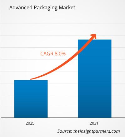
The advanced packaging market was worth ~US$ 30 billion in 2021; it is expected to grow at a CAGR of 8% to reach US$ 55 billion by 2031. There has been a paradigm shift in the packaging/assembly business in recent times. Although Outsourced Semiconductor Assembly and Tests (OSATs) and Integrated Device Manufacturers (IDMs) have been the key contributors to the market for a long, players with different business models including foundries, substrate/Printed Circuit Board (PCB) suppliers, and Electronic Manufacturing Service (EMS) companies are entering into the assembly/packaging business.
Innovations in packaging technology, miniaturization of devices, and increasing adoption of MEMS expected to propel advanced packaging market growth
Innovations in packaging technologies, and focus on heterogeneous integrations and wafer-level packages have prompted the chip industry to develop a new set of solutions, collectively known as advanced packaging. An increase in the size of silicon from 100 mm to 300 mm is a significant trend affecting the advanced packaging market. The shift to wafers with longer diameters has reduced the manufacturing cost by 20-25%. The miniaturization of devices and increasing adoption of MEMS are bolstering the demand for embedded die packaging. Though the technology is not new in the market, the adoption has been limited to niche applications due to high cost and low yield; however, it has immense potential for development in the future. Advancements in the Bluetooth and radiofrequency (RF) modules and the rise of Wi-Fi 6 could further fuel the advanced packaging industry. The continuous evolution of smartphones and tablets technologies, wireless communications, etc., will positively impact the progress of this industry.
Advanced packaging technology to hold more than 60% share in semiconductor packaging market by 2031
The advanced packaging industry held ~40% share in the semiconductor packaging market in 2021, and currently, the market is dominated by traditional packaging platforms. However, advanced packaging technologies are expected to account for more than 60% of the semiconductor packaging market by 2031.

- This FREE sample will include data analysis, ranging from market trends to estimates and forecasts.
The back-end process of supply chains requires significant investments in specialized facilities. Firms specializing in assembly, packaging, and testing typically invest ~15% of their annual revenues in facilities and equipment. The back-end process is relatively less capital-intensive and employs more labor than the front-end fabrication process; however, innovations in advanced packaging are changing these dynamics. Overall, backend process activity accounted for ~14% of the total industry capital expenditure and contributed to ~6.5% of the total value added by the semiconductor packaging industry in 2021. The industry is concentrated primarily in Taiwan and mainland China, and several new facilities are also being built in Southeast Asia (Malaysia, Vietnam, and the Philippines).
Traditional packaging Vs. advanced packaging market trend
The traditional packaging market dominated the overall semiconductor packaging market in 2021. In terms of 300mm equivalent wafer, traditional packaging still dominates with ~72% of the market share. However, advanced packaging is estimated to increase its share of wafers to more than 60% by 2031. The value of advanced wafer packaging is almost double that of traditional packaging, resulting in a high profit margin for semiconductor manufacturers. Flip-chip constituted ~80% of the advanced packaging market in 2021, and it will continue to contribute to a significant market share by 2031.
Technology trends:
- Heterogeneous integration is a key to semiconductor innovation.
- Advanced packaging is seen to raise the value of a semiconductor product, adding functionality and maintaining/increasing performance while lowering cost.
- Various multi-die packaging methods (SiP) are being developed in both high end and low end application for consumer, performance, and specialized applications.
Supply chain:
- The semiconductor manufacturing supply chain is changing at various levels.
- IC substrate and PCB manufacturers—SEMCO, Unimicron, AT&S, Shinko, and so on are entering into the advanced packaging area.
- OSATs are expanding their testing expertise, while traditional pure testing service players are investing in assembly/packaging capabilities.
- TSMC, Intel, and Samsung have emerged as the key innovators of new advanced packaging technologies.
Flip-chip advance packaging platform dominated advanced packaging market in 2021
Among all advanced packaging platforms, 3D/2.5D stacking and fan-out are expected to grow at ~22% and 16% CAGR, respectively from 2021 to 2031. The adoption of such packaging platforms will continue to surge across various applications. Mainly led by mobile phone segment, the market for fan-in wafer-level packaging (FIWLP) will grow at a CAGR of 5% during 2021–2031. Though small (~US$ 50 million in 2021), the embedded die market is expected to grow at a 20% CAGR from 2021 to 2031, and the telecommunications and infrastructure, automotive, and mobile sectors would be the major adopters of this advanced packaging platform.

- This FREE sample will include data analysis, ranging from market trends to estimates and forecasts.
Fan-out wafer level packaging expected to witness significant growth rate
Fan-out wafer-level packaging (FOWLP) has emerged as a promising technology to meet the ever-increasing demands for consumer electronics. This type of packaging benefits through specific features such as substrate-less package, lower thermal resistance, and higher performance. The enhanced performance delivered by FOWLP is attributed to shorter interconnects and direct IC connection by thin-film metallization, instead of the standard wire bonds or flip-chip bumps, and more moderate parasitic effects.
Investment Outlook: Significant investments by IDMs in advanced packaging technology to boost their foundry business
TSMC earned ~US$ 3.6 billion as advanced packaging revenue in 2021. The company announced an estimated US$2.8 billion CapEx in 2021 for its advanced packaging business, geared explicitly toward SoIC, SoW, and InFO variants, and CoWoS product lines. Further, Intel’s investment in various advanced packaging portfolios—such as Foveros, EMIB, and Co-EMIB—is a key to implementing its IDM 2.0 strategy as unveiled by the company's new leadership. The company plans to capitalize on external and internal manufacturing resources to focus on design wins and increased market share, thereby growing Intel’s leadership in the client and data center domains.
Samsung is aggressively investing in advanced packaging technologies to boost its foundry business and emerge as a solid alternative for TSMC. On the other hand, various OSATs are also investing heavily in advanced packaging technologies to compete in the lucrative market. Their CapEx spending increased 27% YoY in 2021 to reach ~US$6 billion, irrespective of the COVID-19 pandemic impact.
Expanding advanced packaging production in us to drive market
With the rise in supply chain concerns and trade tensions, the US is taking the first steps toward bringing larger-scale IC packaging production capabilities back to the country. The country lacks larger-scale packaging production capabilities, substrates, and wafer bumping services. Amkor, Intel, and other companies in the US are making efforts for addressing these issues. While the US is a leader in chip design, it has seen a decline in new fabs and capacity. A large percentage of fab capacity is concentrated in Asia. Nevertheless, Intel, Samsung, TSMC, and others are building new fabs in the US. Thus, chip manufacturing is critical for maintaining technological leadership, both from a supply chain and economic perspective, and for supply chain security reasons.
A few of the notable developments in the advanced packaging industry in the US are as follows:
- Intel is developing an advanced packaging operation in New Mexico.
- SkyWater is developing advanced packaging capabilities in Florida.
- Amkor is looking at building its first plant in the US, while other OSATs are expanding.
- Northrop Grumman will open a packaging processing line in the country.
- The US government has proposed a plan worth US$ 52 billion to boost semiconductor manufacturing in the country, which also involves advanced packaging.
Competitive Landscape: Top 10 players account for more than 70% market share
Intel and Samsung (IDMs); TSMC (a foundry); ASE, SPIL, Amkor, PTI, and JCET (the Top 5 global OSATs); Nepes; and Chipbond are the 10 players that account for ~75% of global advanced packaging industry. The advanced packaging market is significantly driven by end user revenue because of the elevated demand for the latest technologies and high-speed gadgets. The companies have gained sustainable competitive advantages through innovations in this market, owing to the growing need for differentiated products for various applications.
- February 2021: Siemens Digital Industries Software announced a collaboration with Advanced Semiconductor Engineering, Inc. (ASE) to evaluate multiple complex integrated circuit (IC) package assemblies and interconnects in a data-robust graphical environment before and during physical design implementation.
- August 2021: Samsung Electronics announced the availability of its silicon-proven 3D IC packaging technology—eXtended-Cube (X-Cube)—for most advanced process nodes.
- May 2021: Synapse Electronique, a Canadian equipment electronics manufacturer and EMS provider, integrated two Universal Instruments Fuzion Platform production lines in its Shawinigan, Quebec facility.
Advanced Packaging Report Scope
| Report Attribute | Details |
|---|---|
| Market size in 2024 | US$ XX million |
| Market Size by 2031 | US$ 55 billion |
| Global CAGR (2025 - 2031) | 8% |
| Historical Data | 2021-2023 |
| Forecast period | 2025-2031 |
| Regions and Countries Covered | North America
|
| Market leaders and key company profiles |
- Historical Analysis (2 Years), Base Year, Forecast (7 Years) with CAGR
- PEST and SWOT Analysis
- Market Size Value / Volume - Global, Regional, Country
- Industry and Competitive Landscape
- Excel Dataset


Report Coverage
Revenue forecast, Company Analysis, Industry landscape, Growth factors, and Trends

Segment Covered
This text is related
to segments covered.

Regional Scope
North America, Europe, Asia Pacific, Middle East & Africa, South & Central America

Country Scope
This text is related
to country scope.
Trends and growth analysis reports related to Electronics and Semiconductor : READ MORE..
- Amkor technology, Inc.
- ASE Technology Holding Co.Ltd
- Intel Corporation
- Taiwan Semiconductor Manufacturing Company
- SPIL
- PTI
- JCET
- NEPES
- CHIPBOUND
- Samsung

 Get Free Sample For