MARKET INTRODUCTION
The e-beam wafer inspection system market has huge development opportunities globally, owing to the mounting appropriation of these systems by semiconductor manufacturers for their high-quality inspection, which is creating profitable opportunities for the E-beam wafer inspection system market in the forecast period.
MARKET DYNAMICS
The increasing requirement for semiconductor wafers subsequently fosters the need for wafer inspection systems is driving the E-beam wafer inspection system market. The lack of awareness about the features of E-beam wafer inspection system may restrain the growth of the E-beam wafer inspection system market. Furthermore, the growing miniaturization of the system is anticipated to create market opportunities for the E-beam wafer inspection system market during the forecast period.
MARKET SCOPE
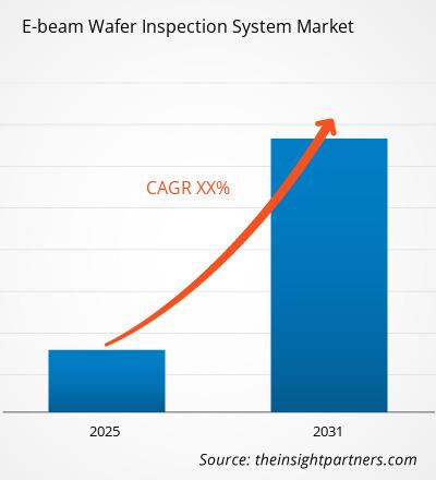
The "Global E-beam wafer inspection system Market Analysis to 2031" is a specialized and in-depth study of the E-beam wafer inspection system market with a special focus on the global market trend analysis. The report aims to provide an overview of E-beam wafer inspection system market with detailed market segmentation by type, application, and geography. The global E-beam wafer inspection system market is expected to witness high growth during the forecast period. The report provides key statistics on the market status of the leading E-beam wafer inspection system market players and offers key trends and opportunities in the E-beam wafer inspection system market.
MARKET SEGMENTATION
The global E-beam wafer inspection system market is segmented on the basis of type, and application. Based on type, the market is segmented into less than 1 NM, 1 to 10 NM, and more than 10 NM. Similarly, on the basis of application the market is segmented into defect imaging, lithographic qualification, bare wafer OQC/IQC, wafer dispositioning, reticle quality inspection, inspector recipe optimization, and others.
REGIONAL FRAMEWORK
The report provides a detailed overview of the industry including both qualitative and quantitative information. It provides overview and forecast of the global E-beam wafer inspection system market based on various segments. It also provides market size and forecast estimates from year 2021 to 2031 with respect to five major regions, namely; North America, Europe, Asia-Pacific (APAC), Middle East and Africa (MEA) and South America. The E-beam wafer inspection system market by each region is later sub-segmented by respective countries and segments. The report covers analysis and forecast of 18 countries globally along with current trend and opportunities prevailing in the region.
The report analyzes factors affecting E-beam wafer inspection system market from both demand and supply side and further evaluates market dynamics effecting the market during the forecast period i.e., drivers, restraints, opportunities, and future trend. The report also provides exhaustive PEST analysis for all five regions namely; North America, Europe, APAC, MEA and South America after evaluating political, economic, social and technological factors effecting the E-beam wafer inspection system market in these regions.
MARKET PLAYERS
The reports cover key developments in the E-beam wafer inspection system market as organic and inorganic growth strategies. Various companies are focusing on organic growth strategies such as product launches, product approvals and others such as patents and events. Inorganic growth strategies activities witnessed in the market were acquisitions, and partnership & collaborations. These activities have paved way for expansion of business and customer base of market players. The market players from E-beam wafer inspection system market are anticipated to lucrative growth opportunities in the future with the rising demand for E-beam wafer inspection system market. Below mentioned is the list of few companies engaged in the E-beam wafer inspection system market.
The report also includes the profiles of key E-beam wafer inspection system market companies along with their SWOT analysis and market strategies. In addition, the report focuses on leading industry players with information such as company profiles, components and services offered, financial information of last 3 years, key development in past five years.
- Applied Materials Inc.
- ASML Holding N.V.
- Hitachi Ltd.
- Integrated Device Technology Inc.
- KLA Tencor Corporation
- Lam Research Corporation
- NXP Semiconductors N.V.
- Renesas Electronics Corporation
- Synopsys Inc.
- Taiwan Semiconductor Manufacturing Co. Ltd.
The Insight Partner's dedicated research and analysis team consist of experienced professionals with advanced statistical expertise and offer various customization options in the existing study.
E-beam Wafer Inspection System Report Scope
| Report Attribute | Details |
|---|---|
| Market size in 2024 | US$ XX million |
| Market Size by 2031 | US$ XX Million |
| Global CAGR (2025 - 2031) | XX% |
| Historical Data | 2021-2023 |
| Forecast period | 2025-2031 |
| Segments Covered |
By Type
|
| Regions and Countries Covered | North America
|
| Market leaders and key company profiles |
- Historical Analysis (2 Years), Base Year, Forecast (7 Years) with CAGR
- PEST and SWOT Analysis
- Market Size Value / Volume - Global, Regional, Country
- Industry and Competitive Landscape
- Excel Dataset


Report Coverage
Revenue forecast, Company Analysis, Industry landscape, Growth factors, and Trends

Segment Covered
This text is related
to segments covered.

Regional Scope
North America, Europe, Asia Pacific, Middle East & Africa, South & Central America

Country Scope
This text is related
to country scope.
Trends and growth analysis reports related to Electronics and Semiconductor : READ MORE..
The List of Companies
1. Applied Materials Inc.
2. ASML Holding N.V.
3. Hitachi Ltd.
4. Integrated Device Technology Inc.
5. KLA Tencor Corporation
6. Lam Research Corporation
7. NXP Semiconductors N.V.
8. Renesas Electronics Corporation
9. Synopsys Inc.
10. Taiwan Semiconductor Manufacturing Co. Ltd.
1. Applied Materials Inc.
2. ASML Holding N.V.
3. Hitachi Ltd.
4. Integrated Device Technology Inc.
5. KLA Tencor Corporation
6. Lam Research Corporation
7. NXP Semiconductors N.V.
8. Renesas Electronics Corporation
9. Synopsys Inc.
10. Taiwan Semiconductor Manufacturing Co. Ltd.

 Get Free Sample For