MARKET INTRODUCTION
Wafer fabrication equipment utilizes chemical & physical processes to generate minute, multi-layer circuits on a round silicon wafers. With growth in the demand for creating circuits for electronic & electrical devices, the scope of wafer fab equipment is rising.
MARKET DYNAMICS
Rising demand for consumer electronics and growth in technological advancements within semiconductor & telecom industry is driving the growth of the wafer fab equipment market. The factors mentioned above are positively impacting the market growth. In addition, IoT is playing a major role in transforming the entire semiconductor industry driven by use of internet connected devices such as smart home and autonomous vehicles. As semiconductors are required in range of cloud integration & connectivity products, need to have more semiconductor wafers is rising which is eventually creating more demand for wafer fab equipment. The trend is expected to fuel the demand for wafer fab equipment during the forecast period.
MARKET SCOPE
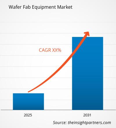
The "Global Wafer Fab Equipment Market Analysis to 2031" is a specialized and in-depth study of the electronics and semiconductor industry with a special focus on the global market trend analysis. The report aims to provide an overview of the wafer fab equipment market with detailed market segmentation - node size, fabrication method, application, and geography. The global wafer fab equipment market is expected to witness high growth during the forecast period. The report provides key statistics on the market status of the leading wafer fab equipment market players and offers key trends and opportunities in the market.
MARKET SEGMENTATION
IMPACT OF COVID-19 ON WAFER FAB EQUIPMENT MARKET
The outbreak of the COVID-19 has negatively impacted the growth of wafer fab equipment market. With temporary shutdown of semiconductor manufacturing plants in different corners of the world, the demand & supply of wafers also got declined. However, with business getting back to normal, the demand for electronics & electrical systems is growing at a decent rate which is also contributing toward the demand for more wafers. This factor will help in boositng the market growth.
REGIONAL FRAMEWORK
The report provides a detailed overview of the industry including both qualitative and quantitative information. It provides an overview and forecast of the global wafer fab equipment market based on various segments. It also provides market size and forecast estimates from the year 2021 to 2031 with respect to five major regions, namely; North America, Europe, Asia-Pacific (APAC), Middle East and Africa (MEA) and South & Central America (SAM). The wafer fab equipment market by each region is later sub-segmented by respective countries and segments. The report covers the analysis and forecast of 18 countries globally along with the current trend and opportunities prevailing in the region.
The report analyzes factors affecting the wafer fab equipment market from both demand and supply side and further evaluates market dynamics affecting the market during the forecast period i.e., drivers, restraints, opportunities, and future trend. The report also provides exhaustive PEST analysis for all five regions namely; North America, Europe, APAC, MEA, and South & Central America after evaluating political, economic, social and technological factors affecting the wafer fab equipment in these regions.
MARKET PLAYERS
The reports cover key developments in the wafer fab equipment market as organic and inorganic growth strategies. Various companies are focusing on organic growth strategies such as product launches, product approvals and others such as patents and events. Inorganic growth strategies activities witnessed in the market were acquisitions, and partnership & collaborations. These activities have paved way for the expansion of business and customer base of market players. The market payers from wafer fab equipment market are anticipated to lucrative growth opportunities in the future with the rising demand for tactile sensors in the global market. Below mentioned is the list of few companies engaged in the wafer fab equipment market.
The report also includes the profiles of key companies along with their SWOT analysis and market strategies in the wafer fab equipment market. In addition, the report focuses on leading industry players with information such as company profiles, components, and services offered, financial information of the last 3 years, the key development in the past five years.
- Applied Materials, Inc
- Advantest
- ASML
- Dainippon Screen Manufacturing Co. Ltd.
- Hitachi Kokusai Electronic Inc
- KLA-Tencor Corporation
- Lam Research Corporation
- Nikon Corporation
- Taiwan Semiconductor Manufacturing Company Limited
- Tokyo Electron Limited
Wafer Fab Equipment Report Scope
| Report Attribute | Details |
|---|---|
| Market size in 2024 | US$ XX million |
| Market Size by 2031 | US$ XX Million |
| Global CAGR (2025 - 2031) | XX% |
| Historical Data | 2021-2023 |
| Forecast period | 2025-2031 |
| Segments Covered |
By Node Size
|
| Regions and Countries Covered | North America
|
| Market leaders and key company profiles |
- Historical Analysis (2 Years), Base Year, Forecast (7 Years) with CAGR
- PEST and SWOT Analysis
- Market Size Value / Volume - Global, Regional, Country
- Industry and Competitive Landscape
- Excel Dataset


Report Coverage
Revenue forecast, Company Analysis, Industry landscape, Growth factors, and Trends

Segment Covered
This text is related
to segments covered.

Regional Scope
North America, Europe, Asia Pacific, Middle East & Africa, South & Central America

Country Scope
This text is related
to country scope.
Trends and growth analysis reports related to Electronics and Semiconductor : READ MORE..
The List of Companies
1.Applied Materials, Inc
2.Advantest
3.ASML
4.Dainippon Screen Manufacturing Co. Ltd.
5.Hitachi Kokusai Electronic Inc
6.KLA-Tencor Corporation
7.Lam Research Corporation
8.Nikon Corporation
9.Taiwan Semiconductor Manufacturing Company Limited
10.Tokyo Electron Limited
1.Applied Materials, Inc
2.Advantest
3.ASML
4.Dainippon Screen Manufacturing Co. Ltd.
5.Hitachi Kokusai Electronic Inc
6.KLA-Tencor Corporation
7.Lam Research Corporation
8.Nikon Corporation
9.Taiwan Semiconductor Manufacturing Company Limited
10.Tokyo Electron Limited

 Get Free Sample For